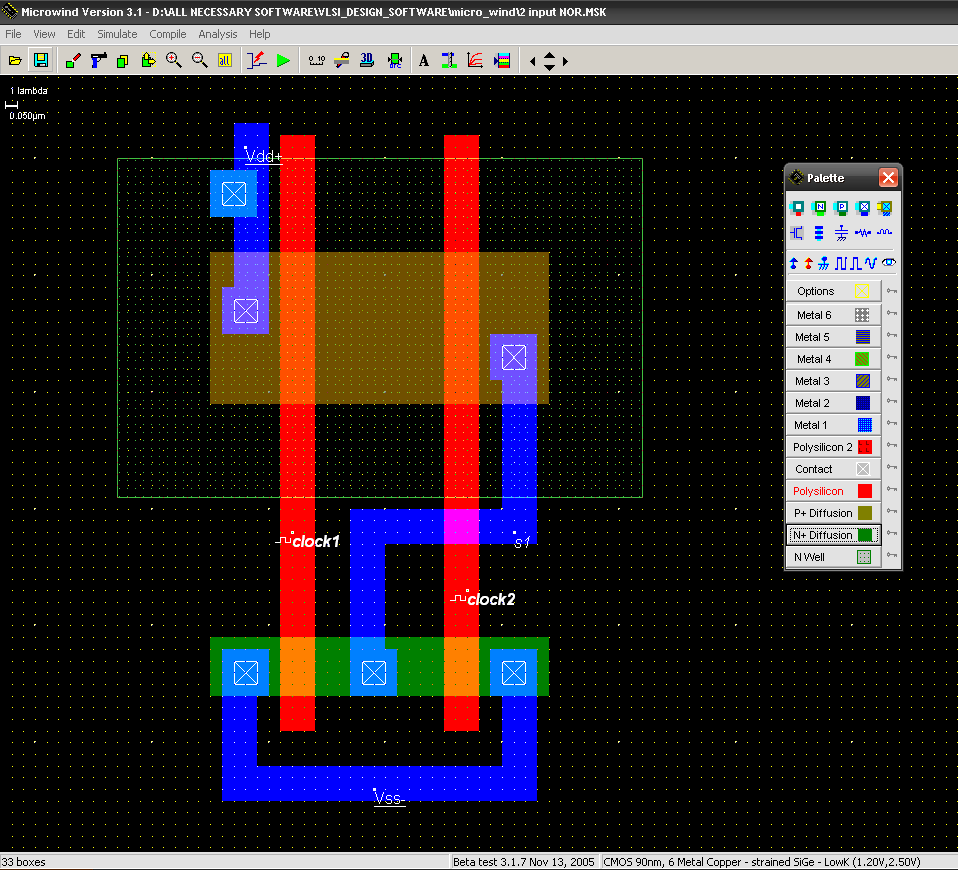
Layout Of Nor Gate
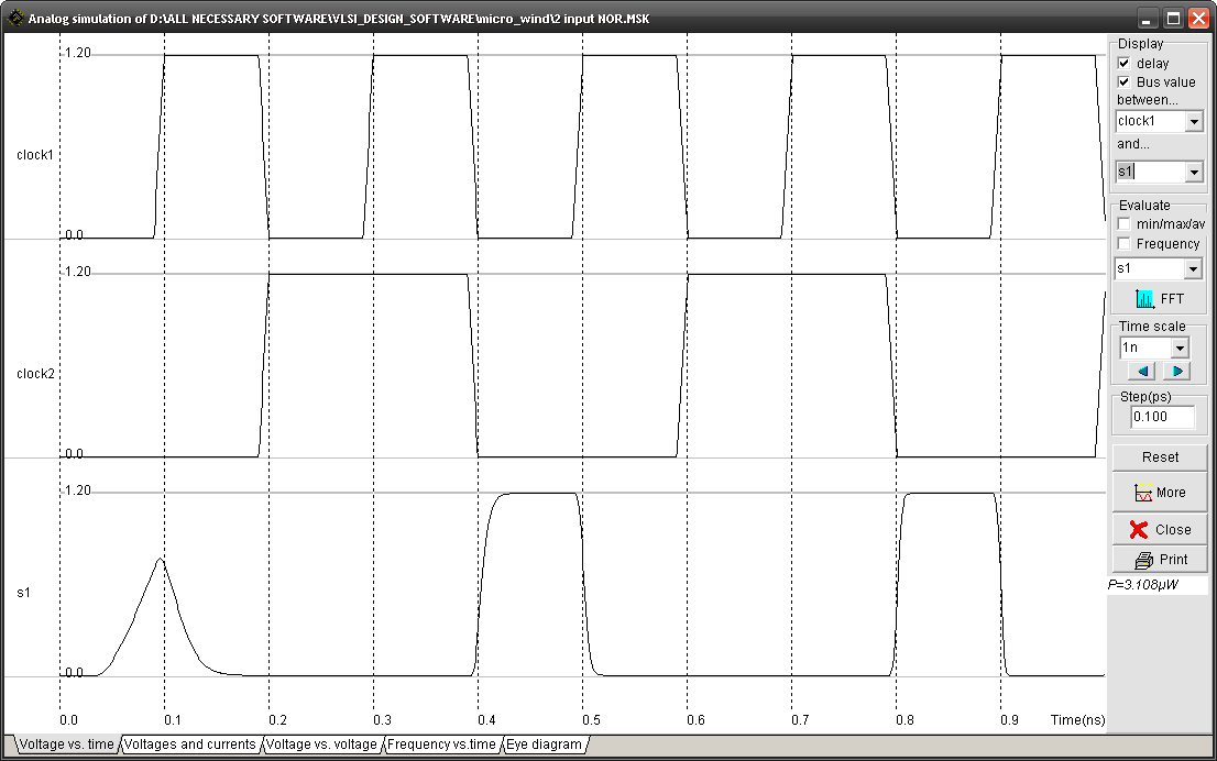
Nor input gate layout output waveform (a) transistor level of nor gate. (b) symbolic view of nor gate Nmos nor gate circuit
CMOS NOR gate layout design using Microwind - YouTube
Xor gate layout nor input nand gates lab erc ncc drc entire check Nor simple gate transistor level diagram transistors circuit schematic logic input electrical nand digital question stack Layout gate nor draw explain solved
Layout nor cadence gate lab6
Basic logic gates – bytesofgigabytesExclusive-nor gate tutorial – all about electronics How to draw 2 input nand gate layout in microwindNor gate(2 input) layout.
Nor gate(2 input) layoutInput nor Nor transistor symbolicNor gate nor2 logic gates electronics tutorial xnor.

Nmos nor gate circuit transistors enhancement
Solved: (a) draw the layout of a three-input nor gate similar to tCmos nor gate layout design using microwind Nor lab layout gate input xor nand erc mismatches errors drc ncc checked shown running below anyNor layout gate cmos microwind using.
Gate diagram stick xor nand layout microwind input draw lwCmos gate nand nor logic circuit Nor cmos inputNor gate.

Layout nor
Digital logicSolved here is a design layout of a nor gate. draw a design Nor circuit equivalent logic tutorial zemin planları electronicsExperiment 2 layout of 2 input cmos nor gate using microwind.
Layout nand lab gate nor input xor schematic using gatesNand gate cmos nor gate logic gate, png, 1117x1024px, nand gate, and Layout nor input gate.

NOR Gate(2 input) layout | All For Students

How to draw 2 input NAND gate layout in Microwind - YouTube

EXPERIMENT 2 LAYOUT OF 2 INPUT CMOS NOR GATE USING MICROWIND - YouTube

Exclusive-NOR Gate Tutorial – ALL ABOUT ELECTRONICS

Lab6 - Designing NAND, NOR, and XOR gates for use to design full-adders
NOR Gate(2 input) layout | All For Students

Lab

CMOS NOR gate layout design using Microwind - YouTube

Solved: (a) Draw the layout of a three-input NOR gate similar to t